Basic Design
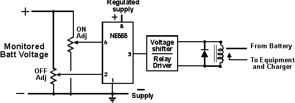 Basic Low Voltage Detector Circuit
Note: There have been some changes since this document was first published. Please note the latest update before constructing the circuit.
Recently in a repeaters owner's discussion group (repeater@repeater.net) reference was made to a "low voltage disconnect circuit" that appeared in QST Nov 93. I made the rash comment that the aforementioned circuit was overly complex and that one could achieve the same ends with a single NE555 IC and a dozen passive components. I was immediately challenged to show this simplified circuit. The following is the result. It does have a few more than a dozen passive parts but still makes a much simpler circuit than the QST article. I hope that it is useful to some folks.
Long Live KISS Design
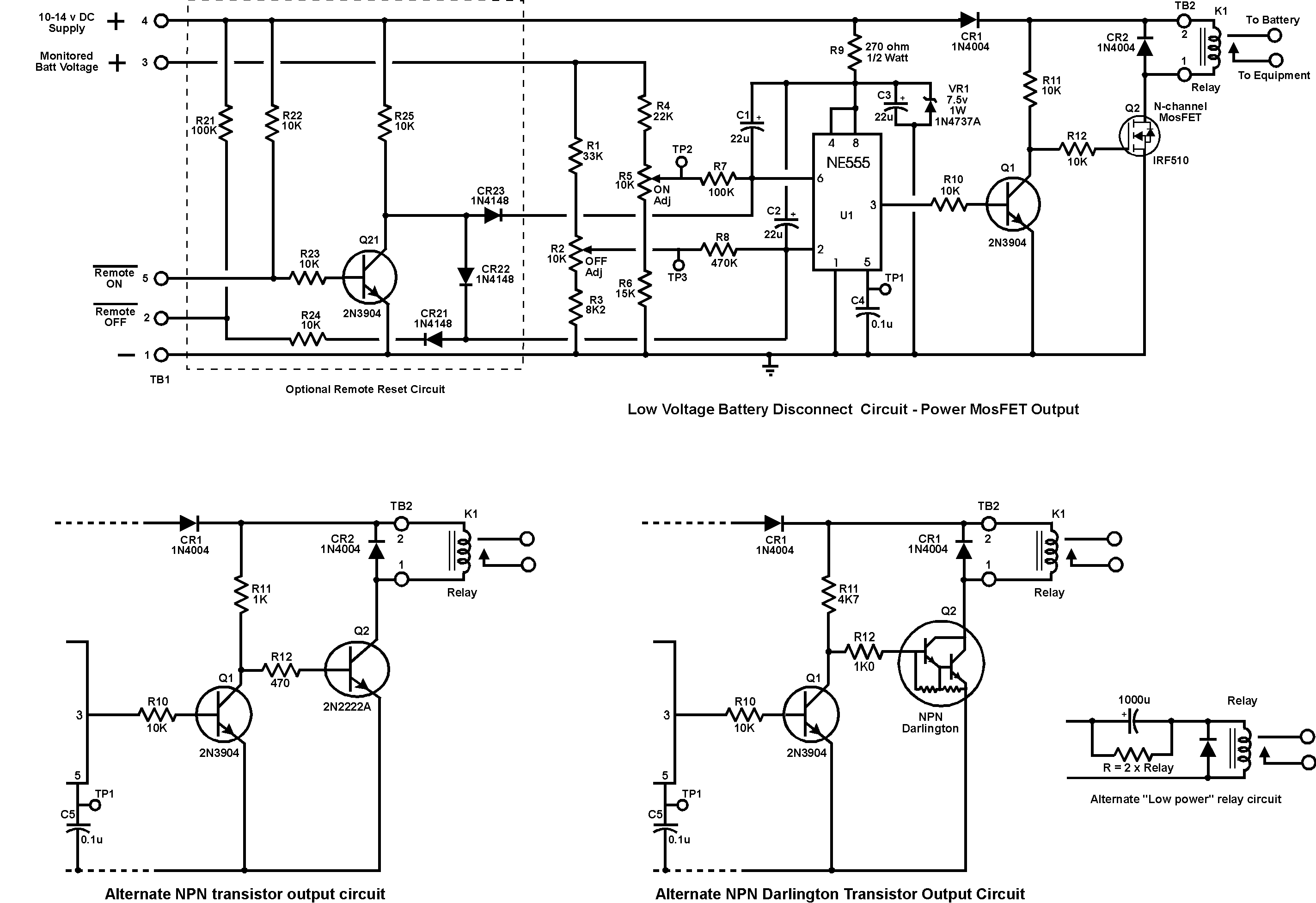
The ubiquitous NE555 "Timer" IC is a very versatile chip. It contains two voltage comparators with an internal reference, an R-S FlipFlop and a "totem-pole" type output circuit capable of sourcing or sinking up to 200 ma. All of these subcircuits are used to advantage in this battery disconnect circuit.
Basically a 555 works as follows:
A pot is connected across the battery to be monitored with the wiper to pin 2 and adjusted so that the voltage on pin 2 equals 1/3 Vcc when the battery is at the desired low voltage disconnect point. When the battery voltage goes below this setpoint, the output voltage on pin 3 will go high.
Another pot is connected across the battery with its wiper to pin 6. It is adjusted so that the voltage on pin 6 is equal to 2/3rds of Vcc when the battery voltage is at the desired "turn-on" setpoint. When the battery exceeds this setpoint, the output pin will go low.
All that is left to enable the disconnect circuit is a relay driver that will turn on the relay when the 555 output is low and release it when the output is high.
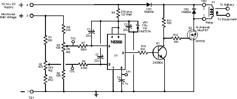
Low Voltage Disconnect Circuit Schematic
U1 (NE555) needs a regulated supply voltage to supply the internal voltage divider references that control the input voltage comparators connected to pins 2 and 6. VR1, a 7.5v 1W zener diode along with R9 dropping resistor is simple and cheap. R9 resistance is chosen so that the zener voltage will be maintained down to about 10v input supply or below. C3 filters the regulated voltage. Should the supply voltage be reversed, the zener diode will clamp the voltage at -0.7v.
The monitored battery voltage input is fed to two voltage dividers, R1, R2 and R3 for the OFF adjustment and R4, R5 and R6 for the ON adjustment. The fixed resistors are chosen so that the pots cover the expected adjustment range (2-3 volts for R2 and 4-6 volts for R5) and make the adjustment easier.
R7 and C1 provide some time delay for the ON adjustment when the monitored voltage abruptly changes. Similarly R8 and C2 provide a time delay for the OFF setpoint for abrupt changes in the monitored voltage. These components have little effect on gradual changes in the monitored voltage but the time delay from abrupt changes depends on the amount of change and how far below the OFF setpoint the lower voltage is. The OFF time delay is about 5 times the ON delay. Since any leakage current in capacitors C1 and C2 will upset the setpoints, they are chosen for minimum leakage.
C1 and C2 capacitors in the time delay circuit also serve another purpose. Conventionally these capacitors would be connected to ground but by connecting them between the input and VCC (U1 regulated supply voltage) the time delay effect is the same and there is an added bonus. When the circuit is powered up, pins 2 and 6 will be forced high momentarily by the charging of C1 and C2 capacitors. This guarantees that the circuit will power up in the "ON" position which is essential for proper operation. If the capacitors were connected to ground, it would power up in the OFF position which would be very undesirable.
U1 pin 5 is connected to one of the internal reference voltage divider taps and C4 filters this point to reduce effects of noise on the power supply. Test point TP1 provides a reference voltage for calibration purposes that can be compared to TP2 (adjust ON Adj so that TP2=TP1) and TP3 (adjust OFF Adj so that TP3=0.5 x TP1).
U1 output pin 3 will have a low voltage when the circuit is "ON" and a high (near VCC) when it has tripped off. Q1 inverts this action so that the "ON" state is high. Q1 and R11 also level shifts the high voltage state to the 10-14 volt supply level rather than the regulated VCC. This reduces the current required from the regulated supply.
CR1 is a protection diode to prevent excessive current flow through the MosFET relay driver if the battery voltage should be reversed.
Q2 is the relay driver. An N-channel power MosFET is the best for this purpose since it requires no current to turn on (only voltage) and can switch considerable power at modest cost. There are alternative relay drivers using NPN single and darlington pair transistors shown below as options. It is also possible to use P-Channel MosFETs as direct "high side switches" in place of the relays. However relays will have the lowest voltage drop (virtually zero) whereas MosFETs have an inherent series resistance RDS that will combine with the current to give a very significant voltage drop. For more details, see the High Side options below.
CR2 protects the circuitry from the reverse spikes that relays generate when they turn off. The relay K1 must be chosen with several factors in mind. You want minimum coil current to conserve power but the relay contacts must be able to handle more than the maximum current that your equipment will draw from the batteries. See "Relay Selection" below. A simple modification to the relay can substantially reduce the current required to hold the relay closed.
A high resolution GIF image of the schematic can be viewed but it may not show or print too well on most browsers. I would recommend that you save it as a file and load it into a bitmap viewer such as PaintShop and print it out from there.
The relay used with this circuit must be chosen with care. On one hand, it must be able to handle the "worse case" current drain expected from the battery. On the other hand, the coil of a large relay generally draws a lot of current and during power outages when the battery is the only source available, the relay can drain the battery all by itself. Even modest relay current can be significant. For example, a relay with a 100 ohm coil will draw 120 ma at 12 volts. Over the space of 24 hours, this will result in a loss of 3 Amp Hour.
A relay that I have found useful for high current is the Potter & Brumfield VF7 series (12v unit p/n = VF7-11F11) with a 70 Amp contact rating and a coil resistance of 72 ohms.
See also the optional relay current reduction circuit below as another way to control relay coil losses.
Don W6OA, Joe K1IKE, Hank N1LTV and possibly others, suggested that a solid state device such as a P-Channel Power MosFET could be used as a relay replacement. That option is discussed below.
There are several options that can be used with the LV Disconnect circuit.
*********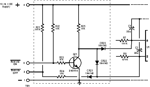
Optional Remote Set/Reset Control Circuit for LV Disconnect
This optional set/reset circuit allows the circuit to be tripped or reset remotely by grounding one of two input pins. This could be useful, for example, on a remote repeater site where there is an alternate control method such as a phone line or a low power control receiver with its own battery. A control signal could reset the disconnect long enough to get a telemetry readout or trip the disconnect even when the battery is still useful in order to save power. I am sure that many more uses for this option can be dreamed up by resourceful users.
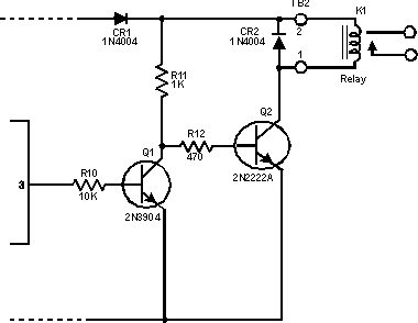
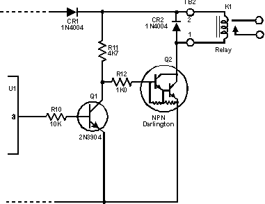
Here are two alternate relay driver circuits using bipolar transistors instead of the power MosFET. I have not checked them out in practice but they should work with the resistor values shown. The 2N2222A should be limited to 350 ma drive current and the darlington to 1 amp maximum.
:*********
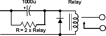
The choice of a suitable relay is difficult. The current needed by the relay can seriously discharge the battery if not chosen with care. Most relays, once they pull in, will hold in with typically 10-25% of their nominal rated voltage. This little circuit will apply full voltage to the relay for long enough to pull it in and then the current will drop to a value just sufficient to hold it in under worse case conditions. The resistor value may have to be experimented with for optimum operation. This should reduce the relay current by 2/3rds or more. The disadvantage is that the relay will not pickup again if it is mechanically opened (such as from a severe mechanical shock or vibration) with the power on. In order to pickup again, the power to it must be cycled. Mechanical dropout would be quite rare (except with human intervention) so this circuit is quite reliable.
Note: A "High Side Switch" is a switch that interrupts power on the positive side of the power supply. Compare this with an NPN transistor or N-Channel MosFET that would control the power on the negative lead by grounding the negative lead of the equipment (the relay driver in the above circuit is such an example). That would be a low side switch. Most 12 volt equipment that we encounter is already negative grounded and a "high side switch" is necessary to switch its power on or off. This distinction applies only to solid state switches where the current can only flow in one direction. Relays do not have this limitation.
Several people including Don W6OA, Joe K1IKE, and Hank N1LTV have suggested that a solid state relay could replace the mechanical relay. This possibility has some notable advantages such as very low actuation current (zero in the case of MosFETs). However all solid state devices have voltage drop either 0.3-0.4 volt in the case of fully saturated bipolar transistors or I x RDS in the case of MosFETs. Since many units designed for 12 volt operation cease working or work in an undesired manner (radios that lose frequency control or generate spurious emissions) when the voltage drops too low (say below 11 volts), the problem of voltage drop in the relay must be very carefully considered. For example, if we consider that the radio should not have less than 11.0 volts applied to it during transmit, the drop in the transistors and wiring could easily exceed 0.5 volt. The battery then should not be allowed to drop below 11.5 volts. But at 11.5v terminal voltage on a lead acid battery, a considerable capacity (30% or more) still remains in the battery that will be wasted.
Personally I consider that 0.2 volts should be the maximum drop in
any "relay" circuit. 0.1 volt drop would be better. That rules
out bipolar transistors. Besides bipolar transistors would need a
continuous base current that would be much more than the coil current in
an equivalently rated relay. What is left? Power MosFETs such as those
made by International Rectifier (IR HexFETs) and Motorola (TMOS FETs).
The key specification that you must look for is the Drain-to-Source
Resistance RDS. This value can vary widely depending on
manufacturer, current and voltage rating, and type
In order to keep the voltage drop low when using P-Channel MosFETs as a high side switch, we have to choose a high current device but only pass low current through it. A number of identical devices connected in parallel would handle higher current. MosFETs are inherently stable when connected in parallel so this configuration should have no surprises. An IRF9540 is rated at 18A and has a RDS of 0.2 ohm so we could not pass more than 1 amp each in order to keep below 0.2v drop. For 10A, we would need 10 devices in parallel. Not too practical.
Again hams to the rescue. Hank, N1LTV, pointed out that
International Rectifier has a P-Channel device with a very low
RDS. The IRF4905 is rated at 50v 64A continuous max with a
RDS of 0.02 ohm. I had not noticed it in my catalogue and
databooks. It is packaged in a TO-220 package and should cost about
$6US in small quantities. Since each device would handle 5-10A and
still have a drop below 0.2v, 10 units in parallel would handle 50-
100Amp at a cost of $60 for the devices. Not cheap, but practical if
your aim is to switch high current without wasting continuous current in
relay coils. That is the key, a relay coil draws current continuously,
many amp hours a day. This solid state switch would have no current draw
continuously and would only lose power as heat
A suggested high side relay circuit using the IRF4905 P-Channel MosFET is shown below. I have not yet checked it out, so if anyone wants to try it, you are on your own. One unknown is the effect on the MosFETs if the supply voltage should be reversed or if the equipment side of the FETs is at a higher voltage than the battery. I will probably order up a quantity of the IRF4905 parts and try them out on a simple circuit board if time permits. Stay tuned for info - but don't hold your breath - blue does not become you :-)
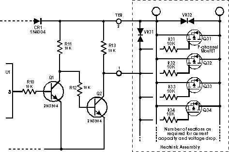
P-Channel MosFET High Side Switch Circuit
This circuit is simple enough that it can be constructed on a perf board. However a printed circuit board is more convenient and neater. A PCB design is shown below.
The components are mostly non-critical and informed substitutions should not be a problem. So far, the only components that I have found to be critical are C1 and C2. These capacitors must have low leakage to avoid affecting the calibration set- points. I have found that tantalum capacitors will be generally suitable but most of the aluminum electrolytic capacitors that I have tried were too leaky. All the tantalum capacitors I tested were better than the best aluminum electrolytic. Sealed axial lead tantalums were the best but dipped (teardrop style) tantalums were also quite good.
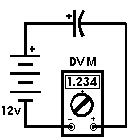
There is a simple test you can use to determine if the capacitors you will be using are suitable. Using a high impedance voltmeter (like 11 Meg input impedance typical of VTVMs and digital voltmeters), you connect the capacitor in series with the voltmeter and a 12 volt battery (capacitor + to battery +). Momentarily short the leads of the voltmeter together (this charges the cap quickly) and then allow the reading to stabilize (it may take several minutes). If the reading is less than 0.5v, the capacitor will be excellent for the job. If the voltage is above 1.0v, there is too much leakage for this circuit application. You can do a final check if the capacitors you are using are suitable during the calibration stage.
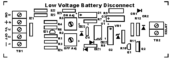
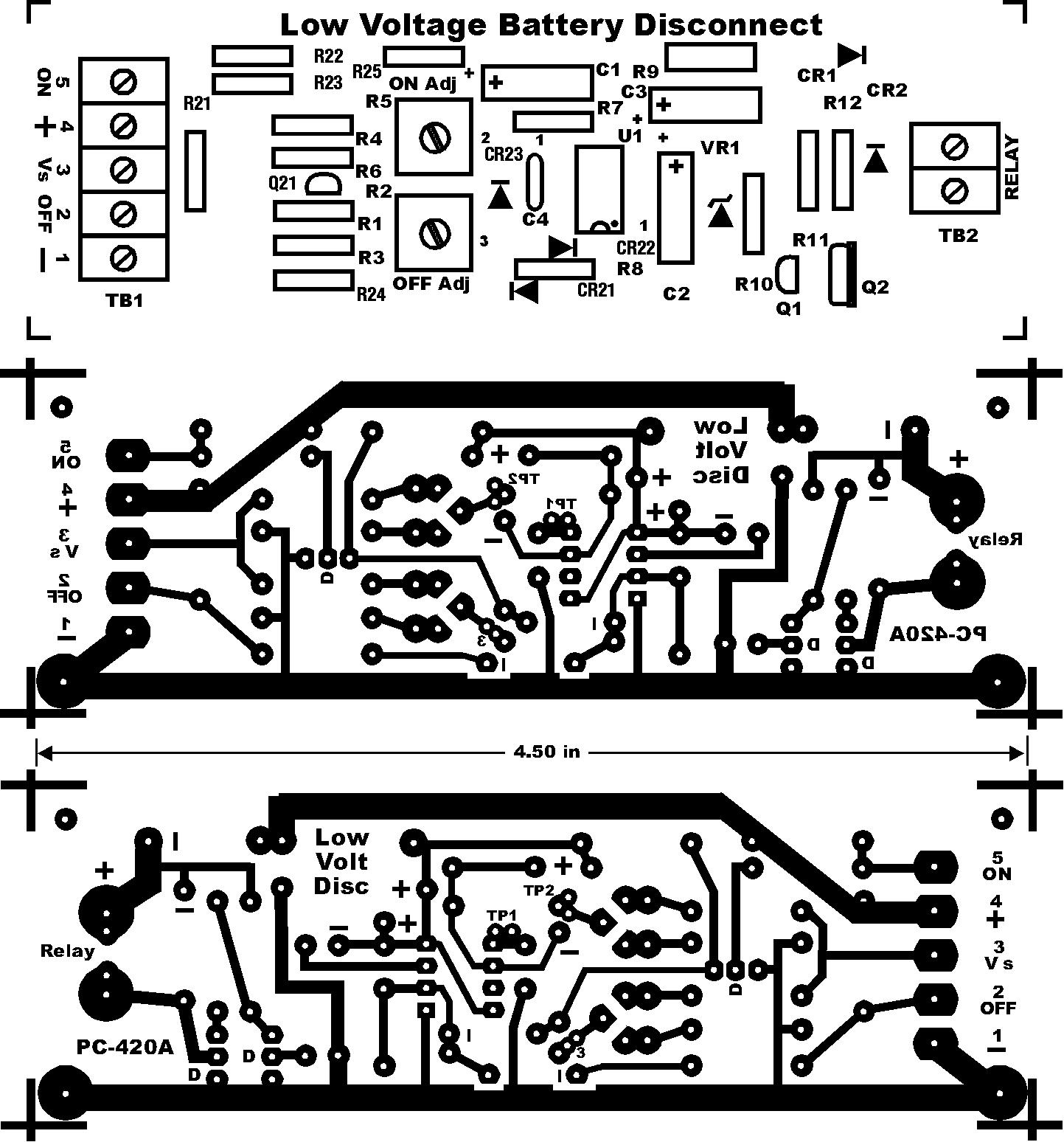
Although terminal blocks are specified for the input and output connections, you can also use solder posts like Vector T-28 (you would have to redrill the holes to 1/16 in dia) or simply wires soldered into the terminal holes. The board is drilled for terminal blocks that are 0.2in (5.08 mm) spacing but 5.00 mm terminals will also fit with no problems. The relay connections (TB2) are also drilled for 3/8 in spaced terminal blocks if you have them.
Since the voltage comparator circuit inputs are high impedance, any leakage from these pins on the IC will cause problems with the calibration set-points. The effect of leaky capacitors C1 and C2 on this problem is discussed above and is verified during calibration. This factor is especially important if the circuit is to be used in an uncontrolled environment where moisture could condense on the board during use. To avoid these problems, the board should be thoroughly cleaned after assembly and testing and then coated on both sides with a thick coating of acrylic lacquer or other suitable insulating material. For PC board cleaning hints, see my document on the subject.
Calibration of this Low Voltage Disconnect circuit is quite simple. You will need a variable power supply that covers both set-point voltages, an accurate high impedance voltmeter preferably digital and a small screwdriver.
The following checks that the electrolytic capacitors C1 and C2 have a suitably low leakage current so that the set points are not affected.
Finally verify the operation as follows:
That completes calibration and circuit verification .
| Designator | Description |
|---|---|
| C1,2 | Capacitor, tantalum electrolytic, low leakage, 22uF, 16-25v |
| C3 | Capacitor, electrolytic, 22uF, 16-25v |
| C4 | Capacitor, ceramic, 0.1 uF, 50v |
| CR1,2 | Diode, silicon, 1 amp, 400 PIV, 1N4004 or equiv. |
| K1 | Relay, 12vDC coil, contacts suitable for application |
| Q1 | Transistor, silicon, NPN, 2N3904 or equiv. |
| Q2 | Transistor, power MosFET, n-channel, 4A, 100v, IRF510 or equiv. |
| R1 | Resistor, carbon film, 33 kilohm, 1/4 watt |
| R2 | Potentiometer, trimpot, 3/8 in square, 10 kilohm |
| R3 | Resistor, carbon film, 8.2 kilohm, 1/4 watt |
| R4 | Resistor, carbon film, 22 kilohm, 1/4 watt |
| R5 | Potentiometer, trimpot, 3/8 in square, 10 kilohm |
| R6 | Resistor, carbon film, 15 kilohm, 1/4 watt |
| R7 | Resistor, carbon film, 100 kilohm, 1/4 watt |
| R8 | Resistor, carbon film, 470 kilohm, 1/4 watt |
| R9 | Resistor, carbon film, 270 ohm, 1/2 watt |
| R10,11,12 | Resistor, carbon film, 10 kilohm, 1/4 watt |
| TB1 | Terminal block, 5 screw terminals, 0.20 (5.00 or 5.08 mm) spacing |
| TB2 | Terminal block, 2 screw terminals, 0.20 (5.00 or 5.08 mm) spacing |
| U1 | Integrated circuit, timer, NE555 |
| VR1 | Diode, zener, 7.5 volt, 1 watt, 1N4737A or equiv. |
| PCB | Printed circuit board, Lantronics PC-420A or equiv. |
| Designator | Description |
|---|---|
| CR21,22,23 | Diode, silicon, switching, 1N4148 or equiv. |
| Q21 | Transistor, silicon, NPN, 2N3904 or equiv. |
| R21 | Resistor, carbon film, 100 kilohm, 1/4 watt |
| R22,23,24,25 | Resistor, carbon film, 10 kilohm, 1/4 watt |
| Designator | Description |
|---|---|
| Q31,32,33,34 | Transistor, power MosFET, p-channel, 55v, 64A, IRF4905 or equiv. |
| R13 | Resistor, carbon film, 10 kilohm, 1/4 watt |
| R31,32,33,34 | Resistor, carbon film, 10 kilohm, 1/4 watt |
| VR21,22 | Suppressor, surge, metal oxide varistor,12vdc, Harris V18ZA1 or Seimens S05K11 |
I have laid out and double checked a printed circuit board for this NE555 based Low Voltage Disconnect. Here is the pattern (PC-420A) for reference purposes. It accommodates all the options except the high side switch option which would have to be mounted on a separate heatsink board. I hope that it shows properly on most browsers. Note that this pattern was modified from the original one (PC-420) published to incorporate necessary circuit changes.
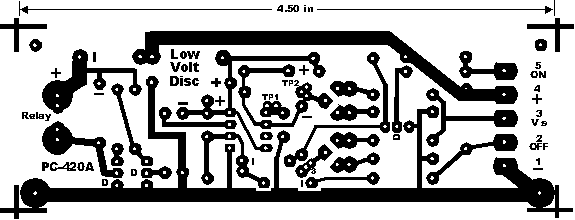
A high resolution (300 dpi) pcb pattern gif image can be downloaded and printed out from a bitmap viewer such as PaintShop. If using this pattern to make your own boards, you must make sure that the pattern is scaled to size properly. Use the size marker to confirm the proper scale
Due to a general lack of sufficient demand for the circuit boards, they are no longer available. A short production run was made 4 years ago but I am no longer in the circuit board business, so they are no longer available from me. You are welcome to use the PCB layouts above to make your own boards if you have the facilities and skill.
You might also be interested in a 12v Battery AmpHour Meter application for this disconnect circuit.
Back to the
Circuits Index
or
Back to
Burt's Home Page
©1998 Burton Lang - All Rights reserved. Revised:28/12/2003